Equilibar valves have a unique design that can benefit processes for front-end-of-line semiconductor fabrication.
Semiconductor manufacturing, particularly the fabrication of integrated circuits (ICs) or “chips”, is one of the most complex industrial processes ever developed. The processors used in our computers, phones, cars, and appliances are produced via a long sequence of manufacturing steps, each requiring ultra-precise engineering, cutting-edge materials science, and nanoscale fabrication techniques.
Given the challenging nature of the manufacturing process, it’s no surprise that Equilibar has helped solve a variety of difficult fluid control problems for our clients. Within these systems, we’ve worked with clients needing extremely precise control, compatibility with incredibly aggressive fluids, and incredibly fast response times. This article describes front-end-of-line processes. See our Back-end-of-line page for descriptions of those processes.
What are the steps involved in chip manufacturing?
Semiconductor fabrication is generally split into three sections: Front-End-of-Line (FEOL), Back-End-of-Line (BEOL), and Advanced Packaging.
- FEOL – the first step in fabrication where individual components like transistors and logic gates are patterned into the wafer substrate
- BEOL –the process in which metal interconnect layers are deposited onto the wafer, connecting the various transistors and other components
- Packaging is the process after chips are sliced from the wafer, when they are then integrated into their final package. Traditionally, this involves encapsulating the chip within a case for protection with electrical contacts that connect to a larger board. (eg. A CPU being packaged in a case with heat spreader and pins to connect to a motherboard) When multiple components are interconnected before traditional packaging/encapsulation, this is referred to as “advanced packaging”. (eg. “chiplets” integrated together onto an interposer board and packaged as a single “chip”).
- Post-fab – final product is integrated into larger components, like a motherboard, server tray, etc. Various tests may be done on the final product, such as thermal stress or performance testing.
Contact Equilibar for More Information
Front-End-of-Line (FEOL) Semiconductor Fabrication
Wafer Surface Preparation
The foundation of most modern ICs is the silicon wafer. These wafers – thin circular slices of a single-crystal ingot of silicon – start as incredibly pure and free of defects in their uniform crystalline lattice structure. Most chips rely on silicon wafers, but some specialized high-power applications use silicon-carbide instead.
Before being processed, these wafers are sliced from the ingot and polished to ensure uniform flatness. This is typically done via chemical mechanical planarization/polishing (CMP) in which a rotating polishing pad along with a chemical slurry are used. CMP is performed prior at the beginning of the process and after many subsequent steps.
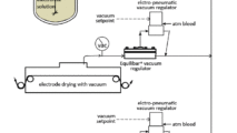
Throughout surface preparation, along with all subsequent steps in the manufacturing process, the silicon wafer is moved from different process chambers via a robotic, automated system. These typically rely on vacuum chucks, which pull vacuum on the bottom surface of the wafer to ensure they are held firmly in place as they are moved about or being operated on. Wafer handling systems often pose a difficult pressure control challenge. As wafers are only a few hundred micron thick, the wafers can be bent or broken if too much vacuum is pulled. Conversely, if not enough vacuum is pulled the wafers will not be securely held and can shift around during the various manufacturing process. Both will lead to loss of the wafer, which can be incredibly costly. A single vacuum chuck could handle different wafers of different diameters as well, leading to variable flow into the system.

Equilibar dome loaded multiple orifice back pressure regulators and vacuum regulators provide extreme precision and responsiveness required for complex semiconductor fabrication applications

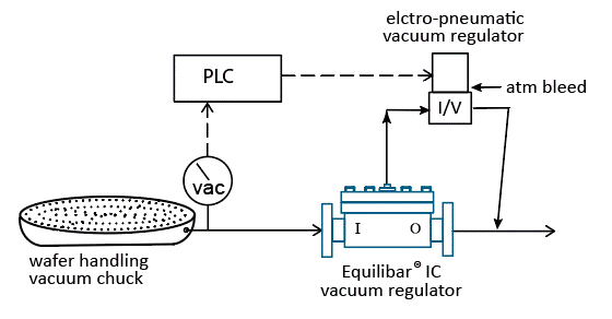
The best solution is to use a vacuum regulator capable of responding quickly to rapid system changes. The Equilibar EVR is designed to immediately open or close when it senses a change in flow, resulting in precise vacuum table pressure control across a wide operating range. With thin polymer diaphragms, our customers can achieve mbar level precision in vacuum wafer handling systems like this. Below is a video demonstrating the responsiveness of the Equilibar EVR in a similar vacuum holding table application.
Why choose Equilibar valves for wafer handling?
- Precise vacuum control – Equilibar vacuum regulators allow for incredibly precise mbar level control, minimizing the risk of damaged wafers
- Wide operating flow range – Equilibar valves have extremely wide turndown ranges spanning 100:1 Cv range or greater, allowing the same valve to be used for different sized wafers/parts without any adjustment of the setpoint
- Fast response – As true regulators, Equilibar valves respond instantaneously to changes in flow and adjust their Cvs accordingly to maintain a constant pressure setpoint. For comparison, a traditional control valve can only adjust its Cv as fast as its control loop can measure a change in pressure and send a command to the positioner; a variable frequency drive on a vacuum pump has the same limitation, in addition to some “wind up” time as it changes speeds. Equilibar valves do not need any external feedback to control upstream pressure.
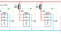
- Isolation from downstream vacuum supply fluctuations – It is very common to have multiple wafer handling machines running in parallel, tied to a shared vacuum header. Other vacuum-based machines pick and place systems or vacuum conveyor belts may use the same shared header, causing the header vacuum level to change as machines start and stop. Equilibar EVR vacuum regulators isolate upstream processes from header fluctuations and adjust their Cv instantaneously to keep that upstream setpoint constant.
- Ease of automation – With an electronic pilot, Equilibar regulators can be easily integrated into automated controls systems.
Once the base substrate layer of the wafer is prepared, subsequent steps follow a circular process of depositing and removing additional layers of material in order to create a complex multi-layered structure of interconnected circuits.

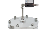
EVR-IC 2″ stainless steel vacuum regulator with manual pilot regulator
Photolithography and Etching
Photolithography is the process by which a circuit is patterned on each layer of a chip. A light sensitive chemical (photoresist) layer is applied to the wafer by spin coating – wherein a small amount of the photoresist is dispensed onto the wafer, which is then spun until it coats the entire surface. The wafer is then exposed to a UV light through a photomask, imparting a circuit pattern. The UV light exposure alters the solubility of the photoresist coating, allowing a solvent (also called a developer) to selectively remove areas leaving only the desired pattern.
Etching is a subtractive process done afterwards in which material is removed by either plasma (dry etching) or chemicals (wet etching) to create the desired structures.
Doping, Annealing and Passivation
The creation of transistors requires some deliberate impurities be introduced into the crystalline lattice structure in a process referred to as “doping”. Elements like Boron, Phosphorous, Arsenic, or Antimony are common dopants for silicon wafers. These dopants are introduced into the lattice structure most commonly via ion implantation – where individual ions are “shot” at the wafer surface via an accelerator. This causes some damage to the surrounding lattice structure though, which must be fixed in order to achieve the desired electrical properties. Most commonly this is done through annealing process in which the wafer is placed in a heated chamber, which allows the lattice to repair itself.
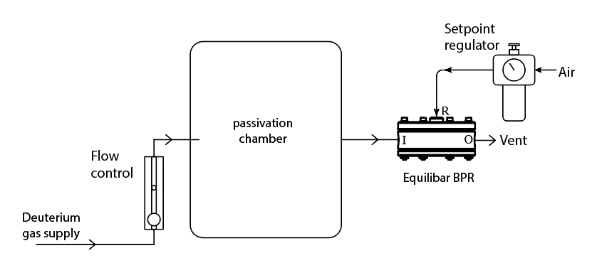
After ion implantation, and other steps in the process that may damage the surface of the silicon wafer and leave “dangling bonds” – silicon atoms without bonding partners. These dangling bonds can impact the electrical properties of the wafer and are typically rectified by hydrogen passivation in which hydrogen bonds with these straggler silicon atoms to patch the lattice structure. This process is similar to annealing, but with the addition of a hydrogen gas blanket in the heated chamber. For high power or advanced chips, sometimes this hydrogen is replaced with its heavier isotope deuterium; the kinetic isotope effect creates a stronger bond with higher activation energy which grants the chip longer lifetime and resistance to high temperatures before the passivation layer fails.
Equilibar BPRs are a great solution for controlling the pressure within annealing/passivation chambers. Within these chambers, temperatures of 250-400 C and gas pressures of 10-30 bar are common. Equilibar’s high temperature valves have a proven track record of allowing for precise pressure control in these challenging conditions across a wide operating flow range. Stable control of pressure within a passivation chamber allows for a faster, more uniform diffusion of hydrogen/deuterium into the wafer.
Why choose Equilibar valves for passivation and annealing chamber control?
- High temperature options – Equilibar valves easily customized for high temperature service, with a polyimide diaphragm and Kalrez o-rings working up to 300 C, metal diaphragms and graphite gasket seals up to 450 C, or all-metal construction with metal c-rings up to 648C.
- Wide operating flow range – Equilibar valves have extremely wide turndown ranges spanning 100:1 Cv range or greater, allowing for precise control within the chamber as the flow into the chamber varies.
- Ease of automation – With an electronic pilot, Equilibar regulators can be easily integrated into automated controls systems.
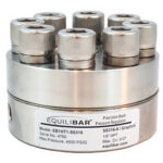
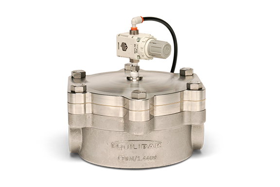
Equilibar HT High Temperature back pressure regulator for high temperature passivation applications